Published configuration: confirm against controlled documents
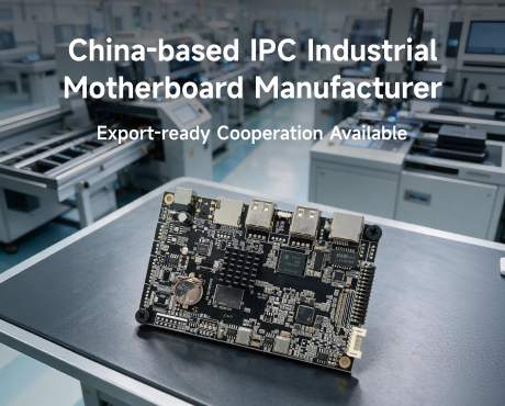
The AS-RK3588-DSG-CUS carrier board is a 6-layer PCB in a 3.5-inch SBC form factor, industrial-grade components throughout, with conformal coating optional. The specifications below are the OEM/ODM default; every line is re-specable on request.
| Block | Specification |
|---|---|
| SoC | Rockchip RK3588 octa-core Cortex-A76/A55 up to 2.4GHz; RK3568 / RK3566 quad Cortex-A55; RK3399; RK3288; Allwinner A133, H618 or T527 on the value tiers |
| NPU | RK3588 6 TOPS INT8; RK3568 1 TOPS; value tiers without NPU |
| GPU | RK3588 Mali-G610 MP4; RK3568 Mali-G52 2EE; A133 PowerVR GE8300 |
| Memory | LPDDR4 / LPDDR4X / LPDDR5, 2GB to 16GB depending on tier |
| Storage | eMMC 5.1 8GB / 16GB / 32GB / 64GB / 128GB; UFS 2.1 option; TF card; M.2 NVMe on the RK3588 carrier |
| Display | Single, dual or triple output: LVDS / eDP / MIPI DSI / HDMI; 1920x1080, 3840x2160 or 7680x4320 decode; independent or mirrored; portrait or landscape per output |
| Touch | Capacitive 10-point / 20-point; dual touch controllers on request; IR touch on request |
| Payment and peripherals | QR / NFC / face payment, barcode imager, thermal printer, cash drawer, weighing scale, RFID, fingerprint, ID card reader |
| Camera | MIPI CSI 2-lane / 4-lane, ISP, 30 fps multi-camera capture for AI SKU recognition |
| I/O | 4x USB 2.0, 2x USB 3.0, RS232 / RS485, up to 6 isolated COM, GPIO island, relay, PWM, I2C, SPI, CAN bus |
| Network | Dual Gigabit Ethernet, PoE+ option, WiFi 5 / WiFi 6, Bluetooth 5.0, 4G LTE / 5G module, SIM slot, 2.4 GHz radio island for ESL |
| OS | Android 11 / 12 / 13 / 14 / 15; Linux; Ubuntu; Debian; AOSP; GMS or GMS-free; kiosk mode |
| Power | 12V DC standard; wide-voltage 9-36V on request; PoE+ on request; hold-up capacitor on request |
| Thermal and reliability | Fanless 6-layer carrier; 0C to 50C standard, -20C to 70C wide temp; 24/7 duty; hardware watchdog; RTC backup; ESD and EMC design |
| Form factor | 3.5-inch SBC, Pico-ITX, Mini-ITX, or core board plus custom carrier |
Application matrix: 8 customization scenarios for the AS-RK3588-DSG-CUS
The AS-RK3588-DSG-CUS is one carrier platform across eight different new retail deployments. The matrix below shows the most common OEM/ODM customization angles an R&D hardware lead in Europe walks through in the first scoping call.
| Scenario | Catalog board limit | AS-RK3588-DSG-CUS customization |
|---|---|---|
| New retail smart terminal | Three BSPs for three store formats | One carrier, one BSP, three formats |
| Smart vending machine | Reference NPU at 11 fps, 8 GPIO | 6 TOPS tuned pipeline, 32-channel island |
| Smart locker controller | 8 GPIO, 1 Hz door poll | 64-channel island, sub-200 ms interrupt |
| Digital signage player | 1080p ceiling, memory leak | 8K decode, 30-day soak-tested loop |
| Dual-screen interactive display | Mirrored output, 400 ms drift | Two framebuffers, sub-16 ms sync |
| Smart shelf gateway | USB radio dongle, blind pushes | On-board 2.4 GHz island, ERP reconciliation |
| Unmanned store terminal | Online-only sales, 4-camera NPU | Signed offline ledger, 12-camera fusion |
| Multi-platform retail family | Four carriers, two contracts | One enclosure, one BSP train, one MOQ |
OEM/ODM workflow: 8 steps from kickoff to first article
Below is the actual OEM/ODM workflow an R&D hardware lead in Frankfurt walks through when commissioning a custom new retail smart terminal Android motherboard from AndroidSBC. No step is a placeholder.
- Day 0-3 — Requirements intake. A 90-minute call captures the store format, the I/O map, the payment stack, the OS choice, the certification scope and the volume profile. Output: a one-page requirements sheet.
- Day 4-7 — Feasibility study. AndroidSBC engineers validate the SoC choice (RK3588, RK3568, RK3566 or A133), the carrier I/O map, the BSP availability, the certification gap and the thermal envelope. Output: a feasibility report with go / no-go on each customization.
- Day 8-12 — Schematic and PCB layout. The AS-RK3588-DSG-CUS carrier board is laid out on a 6-layer stack-up with the customer's I/O map. Output: schematic and PCB review package.
- Day 13-18 — BSP porting. Android, Linux, Ubuntu or Debian BSP is ported to the customer's OS choice, with PREEMPT_RT patches and kiosk-mode locking where needed. Output: a BSP build for the customer's evaluation team.
- Day 19-23 — Sample fabrication. Five to ten engineering samples are fabricated at the Shenzhen source factory, with conformal coating and stencil rework as required. Output: samples shipped to the customer by air.
- Day 24-28 — Customer evaluation. The customer's evaluation team runs thermal, EMC, payment-peripheral and field-replication tests. Output: an evaluation report with sign-off or change requests.
- Day 29-30 — Design freeze and mass-production tooling. Any change requests are absorbed, the design is frozen, and mass-production tooling is opened at the source factory. Output: a frozen Gerber and a frozen BOM.
Thirty-one days from kickoff to first article. Ninety days from kickoff to mass production. This is the OEM/ODM rhythm that the R&D hardware lead in Europe learns to expect from a Shenzhen source factory that does this work for a living.
Frequently asked questions
What is the MOQ for a custom new retail smart terminal Android motherboard?
Answer: 150 units for OEM (a re-spin of an existing carrier board), 500 units for ODM (a from-scratch PCB layout). Sample orders of five units are accepted with an engineering report.
How long does OEM/ODM customization take from kickoff to first article?
Answer: 31 days on the workflow described above, including schematic, PCB layout, BSP porting, sample fabrication and customer evaluation. Mass production starts around day 90.
Should I choose RK3588 or RK3568 for a new retail terminal?
Answer: RK3588 for AI vision, multi-camera SKU recognition, 8K decode and triple independent display; RK3568 for interactive terminals, lockers and gateways where 1 TOPS and 4K dual display are sufficient; A133, H618 or T527 for shelf-edge screens and cost-driven tiers. AndroidSBC builds all of them on the same enclosure cut-out.
Can you drive multiple screens with independent content?
Answer: Yes. Up to three independent outputs on the RK3588 carrier with per-screen resolution, refresh and rotation, independent LVDS and eDP clock domains, sub-16 ms frame sync, and optional dual touch controllers.
Do you support electronic shelf label gateways?
Answer: Yes. An on-board 2.4 GHz radio island driving up to 4,000 labels inside 90 seconds, ERP reconciliation before every write, signed over-the-air updates and a stale-price alarm.
Can you control a smart locker bank from one board?
Answer: Yes. A 64-channel isolated GPIO island with per-door current sensing, 500,000-cycle relay drivers, a hardware tamper interrupt with sub-200 ms latency and a power-fail-safe audit log.
What certifications can you pre-scope for our market?
Answer: CE / FCC / RoHS standard. UL / UKCA / KC / PSE / SAA, GMS / Google EDLA, EMVCo L2 and PCI PTS are all pre-scoped on request. EMC pre-scanning is done in-house before third-party testing.
Do you support OEM/ODM and private label?
Answer: Yes. Custom logo, custom firmware, custom boot animation, custom UI, private-label PCBA and custom SDK modules are all standard OEM/ODM deliverables.
Do you accept sample and small-batch orders?
Answer: Yes. Samples ship in 1-3 days from stock where available; custom samples ship inside the 19-23 day window. Small-batch and large-volume pricing is available on request.