Published configuration: confirm against controlled documents
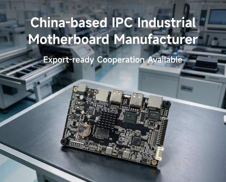
The AS-RK3588-PC-CUS carrier board is a 6-layer PCB, 170 mm x 110 mm (3.5-inch SBC form factor), industrial-grade components throughout, conformal coating optional. The specifications below are the OEM/ODM default; every line is re-specable on request.
| Block | Specification |
|---|---|
| SoC | Rockchip RK3588, octa-core (4x Cortex-A76 2.4GHz + 4x Cortex-A55 1.8GHz), 8nm |
| NPU | 6 TOPS INT8, triple-core, INT4/INT8/INT16 mixed precision |
| GPU | Mali-G610 MP4, OpenGL ES 3.2 / Vulkan 1.2 / OpenCL 2.2 |
| Memory | LPDDR4/LPDDR4X 4GB / 8GB / 16GB / 32GB; LPDDR5 on request |
| Storage | eMMC 32GB / 64GB / 128GB; M.2 NVMe; SATA 3.0; concurrent option |
| Display | HDMI 2.1 (8K@60fps), DP 1.4, LVDS / eDP / MIPI, 7-screen independent display on request |
| Camera | 2x / 4x / 8x MIPI CSI lanes, ISP 48MP, multi-camera input |
| Network | Dual GbE (with PoE+ option), WiFi 6 802.11ax, Bluetooth 5.3, 4G / 5G module |
| Industrial I/O | CAN FD, RS232 / RS485 (isolated), 4x COM ports on request |
| Expansion | PCIe 3.0 x4, M.2 NVMe, SATA 3.0, USB 3.0 host |
| OS | Android 12 / 13 / 14 / 15; Android TV 14; Ubuntu 22.04 LTS; Debian 12; OpenHarmony 4.0 |
| Power | 12V DC standard; wide-voltage 9-36V on request; 24V vehicle + 60V load-dump on request |
| Thermal | Fanless 6-layer PCB; -40C to 85C industrial; conformal coating optional |
Application matrix: 8 customization scenarios for the AS-RK3588-PC-CUS
The AS-RK3588-PC-CUS is the same carrier board across 8 different ARM PC / mini-PC / NAS / set-top box board deployments. The matrix below shows the most common OEM/ODM customization angles a R&D hardware lead in Europe walks through in the first scoping call.
| Scenario | Catalog board limit | AS-RK3588-PC-CUS customization |
|---|---|---|
| Edge AI inference box | 4 GbE, 2 SATA, no PoE | 8 GbE, 4 SATA, 8-port PoE+ |
| AGV / AMR / service robot | No CAN FD, no EtherCAT | CAN FD + 100BASE-T1 + EtherCAT |
| Machine vision inspection | 2 MIPI CSI lanes | 8 MIPI CSI lanes + PoE+ |
| 16-channel AI NVR | 4-channel AI quota | 16-channel AI + RAID-6 BSP |
| Smart cockpit 7-screen | 3 screens, CAN 2.0B | 7 screens, CAN FD, 24V vehicle |
| 8K video-wall signage | 2 screens, fan-cooled | 4 screens, fanless, IP65 |
| Self-service kiosk | 2 COM, GMS-baked AOSP | 8 isolated COM, GMS-free AOSP |
OEM/ODM workflow: 8 steps from kickoff to first article
Below is the actual OEM/ODM workflow a R&D hardware lead in Madrid walks through when commissioning a custom RK3588 motherboard from AndroidSBC. No step is a placeholder.
- Day 0-3 — Requirements intake. A 90-minute call captures the deployment profile, the I/O map, the OS choice, the certification scope, and the volume profile. Output: a one-page requirements sheet.
- Day 4-7 — Feasibility study. AndroidSBC engineers validate the SoC, the carrier board I/O map, the BSP availability, the certification gap, and the thermal envelope. Output: a feasibility report with go / no-go on each customization.
- Day 8-12 — Schematic + PCB layout. The AS-RK3588-PC-CUS carrier board is laid out on a 6-layer stack-up with the customer's I/O map. Output: schematic + PCB review package.
- Day 13-18 — BSP porting. Android / Linux / Ubuntu / OpenHarmony BSP is ported to the customer's OS choice, with PREEMPT_RT patches where needed. Output: BSP build for the customer's evaluation team.
- Day 19-23 — Sample fabrication. 5 to 10 engineering samples are fabricated at the Shenzhen source factory, with conformal coating and stencil rework as required. Output: samples shipped to the customer by air.
- Day 24-28 — Customer evaluation. The customer's evaluation team runs thermal, EMC, reliability, and field-replication tests. Output: evaluation report with sign-off or change requests.
- Day 29-31 — Design freeze + mass-production tooling. Any change requests are absorbed, the design is frozen, and mass-production tooling is opened at the source factory. Output: a frozen Gerber + a frozen BOM.
Thirty-two days from kickoff to first article. Ninety days from kickoff to mass-production. This is the OEM/ODM rhythm that the R&D hardware lead in Europe learns to expect from a Shenzhen source factory that does this work for a living.
Frequently asked questions
What is the MOQ for a custom RK3588 motherboard?
Answer: 100 units for OEM (re-spin of an existing carrier board), 500 units for ODM (from-scratch PCB layout). Sample orders of 5 units are accepted with an engineering report.
How long does OEM/ODM customization take from kickoff to first article?
Answer: 32 days on the OEM/ODM workflow described above, including schematic, PCB layout, BSP porting, sample fabrication, and customer evaluation.
What OS does the BSP support?
Answer: Android 12 / 13 / 14 / 15; Android TV 14; Ubuntu 22.04 LTS with PREEMPT_RT patches; Debian 12; OpenHarmony 4.0. Custom OS ports on request.
What certifications can you pre-scope?
Answer: CE / FCC / RoHS standard. UL / UKCA / KC / PSE / SAA, GMS / Google EDLA, EMVCo L2, PCI PTS 6, EN 50155, E-Mark — all pre-scoped on request.